

Prototype PCB From Environmental Damage
PCBs play an essential role in modern electronic devices, including smartphones, tablets and cars. They enable these products to work at higher speeds and perform more functions than ever before. However, as technology evolves, PCBs are increasingly exposed to environmental damage and other threats that can cause a variety of problems. Moisture, for example, can corrode the copper areas of a circuit board and result in faulty connections and even failure. Other environmental factors such as dust, temperature fluctuations and electromagnetic interference can also negatively affect a prototype PCB’s performance.
As such, it is vital to protect a prototype PCB from environmental damage. There are several effective strategies for doing so, such as encapsulating the PCB or placing it in an enclosure. However, the most effective solution is a conformal coating that protects the circuit board from moisture, fluids, contaminants and other harmful agents.
The most common way to protect a PCB from moisture is by encapsulating it in resin. This process involves putting an assembled PCB inside of a container in which resin is poured to fully encapsulate the circuit board. However, this method offers only a limited level of protection as the resin layer may not completely cover every component on the circuit board. Additionally, the surface of the resin layer can become contaminated with dirt or fingerprints, which may reduce the level of protection offered by the encapsulation.
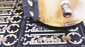
How to Protect a Prototype PCB From Environmental Damage
A conformal coating is a thin polymer film that is applied to the PCB and its components. It is designed to adhere to the surfaces of the circuit board and its components, providing a protective barrier against moisture, oils, fingerprints, dirt and other environmental contaminants. The coating can also prevent corrosion by shielding the conductive traces and other metal parts of the circuit board from moisture, fluids, dust and other harmful agents.
One of the most important things to do to protect a fast-turnaround PCB is to ensure that it is not exposed to electrostatic discharge (ESD). ESD damage can be extremely harmful to sensitive electronic components and can result in damaged or failed prototype printed circuit board assembly, delayed project timelines and lost revenue.
To avoid ESD damage, it is crucial to create a controlled environment in which the PCB will be stored, inspected and tested. This can be done by ensuring that the workspace is grounded through an ionizer or anti-static mat, and by designating specific areas for assembly, testing and storage of the PCBs. It is also a good idea to use a certified ESD tester to evaluate the sensitivity of each prototype to ESD stress and to identify any weak points in the design.
As technology continues to advance, it is important to protect your fast-turnaround PCB prototypes from environmental damage. Taking steps to do so can help you save time, money and resources by avoiding expensive and time-consuming repairs or replacements. By following these tips, you can be sure that your fast-turnaround PCBs will have the best possible chance of functioning properly and efficiently.
