measures are taken to prevent solder balling during Pcb rigid flex
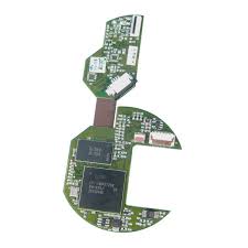
Preventing solder balling during PCB rigid flex assembly is crucial for ensuring the reliability and functionality of electronic devices. Solder balling, also known as solder bridging or solder splashing, occurs when solder material forms unintended connections between adjacent pads, traces, or components during the soldering process. This defect can lead to short circuits, electrical malfunction, and compromised assembly integrity. Addressing solder balling requires a combination of design considerations, process controls, and quality assurance measures.
One of the primary measures taken to prevent solder balling is optimizing solder paste deposition. Consistent solder paste volume, stencil thickness, and aperture design ensure uniform solder joint formation, minimizing the risk of excess solder material that can contribute to solder balling. Advanced stencil technologies, such as laser-cut or nano-coated stencils, provide enhanced control over solder paste deposition, improving soldering consistency and reducing the likelihood of solder balling defects.
Furthermore, controlling reflow soldering parameters is essential for mitigating solder balling risks. Proper temperature profiling, including temperature ramp rates, peak temperatures, and time-above-liquidus (TAL) values, influences solder paste reflow and component soldering. By optimizing these parameters based on the specific requirements of pcb rigid flex assemblies, manufacturers can minimize the occurrence of thermal gradients and solder splashing phenomena that contribute to solder balling defects.
What measures are taken to prevent solder balling during Pcb rigid flex?
Additionally, implementing nitrogen reflow or vacuum reflow atmospheres can help prevent solder balling by minimizing the formation of voids and promoting better wetting between solder paste and component leads. These controlled atmospheres create a more stable soldering environment, reducing the likelihood of solder balling defects and improving overall assembly quality and reliability.
Moreover, proper component placement and design play a significant role in preventing solder balling during PCB rigid flex assembly. Symmetrical component designs, balanced pad layouts, and adequate spacing between components help distribute solder paste and thermal energy evenly during reflow soldering, minimizing the risk of unequal forces that can cause solder balling. Additionally, avoiding large thermal mass imbalances and ensuring proper alignment of components further reduce the likelihood of solder balling occurrences.
Implementing robust quality control measures is essential for detecting and mitigating solder balling defects during PCB rigid flex assembly. Automated optical inspection (AOI) and X-ray inspection systems enable early detection of solder balling defects, allowing for prompt corrective actions to be taken. By conducting thorough inspections throughout the assembly process, manufacturers can identify and address solder balling issues before they impact the functionality and reliability of the final product.
Furthermore, continuous process optimization and refinement are essential for preventing solder balling in PCB rigid flex assembly. By analyzing soldering data, monitoring process parameters, and implementing corrective actions, manufacturers can identify potential sources of solder balling defects and implement preventive measures to address them proactively. This iterative approach to process improvement ensures ongoing quality and reliability in PCB manufacturing operations.
In conclusion, preventing solder balling during PCB rigid flex assembly requires a comprehensive approach that encompasses design optimization, process control, quality assurance, and continuous improvement. By optimizing solder paste deposition, controlling reflow soldering parameters, ensuring proper component placement and design, implementing robust quality control measures, and continuously refining assembly processes, manufacturers can minimize the risk of solder balling defects and ensure the reliability and functionality of electronic devices.