
Blind Vias in High-Speed PCB Routing
Incorporating blind vias in PCBs can improve signal performance and reduce overall board size. This technology is used in high-speed communication and consumer electronics products. However, it is important to understand the limitations of these vias before incorporating them into your design. In this blog post, we will discuss the role blind via pcb play in high-speed PCB routing, and discuss some of the factors that can affect their manufacturability.
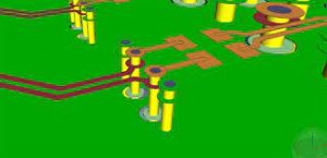
Blind and buried vias are small holes in a printed circuit board that provide connections between layers. These vias are typically used in high-density interconnect (HDI) PCB designs, and they can help to reduce signal interference and EMI between traces on the same layer. In addition, blind and buried vias can reduce the number of layers needed to accommodate components in a PCB, which can help to lower costs.
While blind and buried vias offer many benefits, they can be challenging to manufacture. They require precise drilling and plating techniques that can increase manufacturing costs. Furthermore, they can cause issues such as air bubbles or short circuits if not designed correctly. To avoid these issues, it is important to follow best practices for using blind and buried vias in your PCB designs.
To prevent air bubbles in a blind via, it is critical to design the location of the hole in the copper layer and its surrounding area properly. For example, it is important to use a smaller hole diameter than the pad size, and to ensure that the hole is fully enclosed by the copper layer.
The Role of Blind Vias in High-Speed PCB Routing
In addition, it is important to make sure that the hole is drilled to the side of the pad rather than directly over it. This will help to prevent the formation of an air bubble that could interfere with signal transmission or contaminate the solder joint.
A common cause of a blind via causing problems is the improper placement of copper pads around the hole. This can result in the formation of a “bad” via, which is characterized by an annular ring that is too small or thick, and may not have adequate connection to the underlying copper layer.
Another common cause of bad vias is the failure to design for sufficient via clearance. This is usually caused by placing the via too close to other features on the board, or by not designing for a sufficiently large capture pad. In either case, this can lead to electrical interference or poor conductivity between the via and its surrounding areas.
In addition to these issues, it is important to consider the aspect ratio of the via when designing for manufacturability. The ratio of the via’s depth to its diameter is critical in determining how well it will work and whether it will encounter any manufacturability issues. A higher aspect ratio can increase the risk of plating defects and reduce signal integrity. This can also make the via harder to locate during assembly.