Components of a PCB Design & Assembly
A Printed Circuit Board is an electronic assembly that connects and controls the electrical components in a device. It is composed of layers of copper or other metals that provide conductor paths through which electrical signals travel. The PCB’s design is based on the physical requirements of the components and how they communicate with one another. It also takes into account any power needs or other environmental concerns for the device.
A PCB’s design & assembly begins with front-end engineering, during which the major components are selected and basic circuit diagrams are created. During this phase, ECAD software converts these schematic diagrams into the physical layout of a PCB. This layout must be carefully arranged to ensure that all connections are correct and that the circuit will function properly.
The layered structure of a PCB allows for greater intricacy and special signal paths. However, the addition of layers can add to the cost of the final product. Therefore, designers must carefully balance the amount of detail with cost constraints. This balance is achieved through a scalability-conscious design.
This means that the layout must be flexible enough to allow for future expansion or modifications without having to re-design the entire board. It also means that the layers must be properly matched to the components’ power needs, as well as other constraints like space limitations and materials availability.
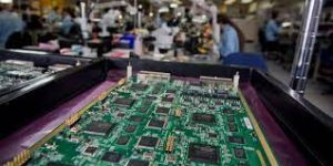
During the PCB fabrication process, the inner layers are fused together using lamination. This creates a solid, cohesive foundation for the rest of the assembly. Next, the drilled holes in the panel are filled with copper through a process called panel plating. This makes them more effective for connecting the different circuit parts.
Key Components of a PCB Design & Assembly
Once the internal layers are prepared, a soldering paste is applied to the surface of the circuit board. Assemblers use a stencil with stainless steel to apply the paste to the areas where components will sit in the finished product. The stencil is designed to prevent contaminating other areas of the circuit board. This step is critical because it can make or break the overall performance of the final product.
The assemblers then solder all the components onto the circuit board. They may also install heat sinks to help the components stay cool and operating effectively. This stage includes using no-clean flux, which is specially formulated to reduce the risk of oxidation and maintain a smooth solder flow.
If the assemblers are assembling sensitive through-hole components, they should include notes in the assembly manual that clearly specify how to handle these parts. For example, the assemblers should use a hand-soldering method instead of wave soldering for these parts to avoid damage to their delicate leads.
The final steps in the pcb design & assembly process involve cleaning the circuit board and testing its functionality. This testing can be conducted by a machine, such as an automated optical inspection (AOI) system, or manually. This test is crucial because it helps to ensure that the finished circuit board functions exactly as the designer intended.